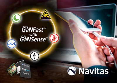
Navitas Introduces Third Generation GaN Power IC with GaNSense™ Technology
Navitas Semiconductor (Nasdaq: NVTS) announced the launch of its third-generation GaN power ICs featuring GaNSense technology. This innovation enhances real-time sensing and protection, improving reliability and efficiency. The new product line includes 10 different ICs, optimized for fast-charging applications with significant energy savings of up to 10% compared to earlier models. Navitas has shipped over 30 million GaNFast power ICs, achieving excessive field operation without failures. The new ICs will be showcased at key industry events and are now in mass production.
- Launch of 10 GaN power ICs with GaNSense technology improves energy efficiency by up to 10%.
- Over 30 million GaNFast power ICs shipped with zero reported field failures.
- Target markets estimated at $2B/year for fast chargers and $2B/year for consumer electronics.
- Enabled faster detection and protection with a response time of 30 ns, significantly enhancing reliability.
- None.
Insights
Analyzing...
EL SEGUNDO, Calif., Nov. 5, 2021 /PRNewswire/ -- Navitas Semiconductor (Nasdaq:NVTS), the industry-leader in gallium nitride (GaN) power integrated circuits ("ICs") has announced the launch of GaNFast™ power ICs with GaNSense technology. GaNSense technology integrates critical, real-time, autonomous sensing and protection circuits which further improves Navitas' industry-leading reliability and robustness, while increasing the energy savings and fast-charging benefits of Navitas' GaN IC technology.
Gallium nitride (GaN) is a next-generation semiconductor technology that runs up to 20x faster than legacy silicon and enables up to 3x more power and 3x faster charging in half the size and weight. Navitas' GaNFast™ power ICs integrate GaN power and drive plus protection and control to deliver simple, small, fast and efficient performance.
GaNSense technology integrates real-time, accurate and fast sensing of system parameters including current and temperature. This technology enables a patent-pending loss-less current-sensing capability, which improves energy savings by up to an additional
With the industry's tightest current-measurement accuracy and GaNFast response time, GaNSense technology means reducing dangerous over-current spikes by
"From detection to protection in only 30 ns, GaNSense technology is
The new family of GaN power ICs with GaNSense technology spans 10 products, which all have the core, critical GaNFast integration of GaN power, GaN drive, control and protection. All are rated at 650V/800V with 2kV ESD protection, and RDS(ON) ranging from 120 to 450 mOhms in 5x6 and 6x8 mm PQFN packaging… with the GaNSense protection circuits and loss-less current-sensing. This family of 3rd generation GaN ICs is optimized for modern power conversion topologies including high-frequency quasi-resonant (HFQR) flyback, active-clamp flyback (ACF) and PFC boost, which are popular to deliver the fastest, most efficient and smallest chargers and adapters within the mobile and consumer markets.
Target markets include fast-chargers for smartphones and laptops, with an estimated GaN potential of
To date, over 30 million GaNFast power ICs have shipped, achieving over 116 billion device hours in the field – with zero reported GaN field failures. Each GaNFast power IC shipped has a 4-10x reduced carbon footprint and saves 4 kg of CO2 compared to legacy silicon chips.
GaNFast power ICs with GaNSense technology will be showcased at the following events:
- 8 November: WiPDA 2021 (virtual) by Dan Kinzer, Navitas COO / CTO and co-founder
- 11 November: CPSSC 2021 (Shanghai) by Dr. Xiucheng Huang, Sr. Director, Applications
- 18 November: PSMA Power Technology Roadmap (virtual) by Dan Kinzer
GaNFast power ICs with GaNSense technology are in mass production with immediate availability. Full technical details of the new GaNSense technology, including datasheets, qualification data, application notes and samples are available to customer partners under NDA.
About Navitas
Navitas Semiconductor (Nasdaq:NVTS) is the industry leader in GaN power ICs, founded in 2014. GaN power ICs integrate GaN power with drive, control and protection to enable faster charging, higher power density and greater energy savings for mobile, consumer, enterprise, eMobility and new energy markets. Over 130 Navitas patents are issued or pending, and over 30 million GaNFast power ICs have been shipped with zero reported GaN field failures. Navitas rang the Nasdaq opening bell and started trading on Nasdaq on October 20th, 2021, with an enterprise value over
Navitas Semiconductor, GaNFast and the Navitas logo are trademarks or registered trademarks of Navitas Semiconductor. All other brands, product names and marks are or may be trademarks or registered trademarks used to identify products or services of their respective owners.
Contact Information
Stephen Oliver, VP Corporate Marketing & Investor Relations
ir@navitassemi.com
![]() View original content to download multimedia:https://www.prnewswire.com/news-releases/navitas-introduces-third-generation-gan-power-ic-with-gansense-technology-301417563.html
View original content to download multimedia:https://www.prnewswire.com/news-releases/navitas-introduces-third-generation-gan-power-ic-with-gansense-technology-301417563.html
SOURCE Navitas Semiconductor


