DNP Develops TGV Glass Core Substrate for Semiconductor Packages
- Contributing to higher performance semiconductors -

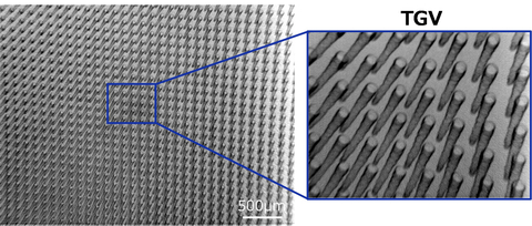
X-ray image of TGV in the glass core substrate (Graphic: Business Wire)
[Features]
• Fine pitch and high reliability
The newly developed GCS includes a TGV necessary for electrically connecting the fine metal wiring configured on the front and back of the glass. It is a Conformal Type glass substrate in which a metal layer is adhered to the side walls of the via. Our new proprietary manufacturing method enhances the adhesion between glass and metal, which was difficult to achieve with conventional technology, to realize fine pitch and high reliability.
• High aspect ratio and large-scale
The newly developed glass substrate has an aspect ratio of 9+, and maintains sufficient adhesive qualities to configure fine wiring. As there are few restrictions regarding the thickness of the glass substrate used, it is possible to boost the degree of freedom when designing warpage, rigidity, and flatness. It is also possible to accommodate package scalability by employing our panel manufacturing process.
[Going Forward]
In addition to the existing Filling Type glass substrate that fills the glass Via with copper, DNP is also promoting the scalability of the newly developed Conformal Type glass substrate to a panel size of 510 x 515mm. We aim for sales of
About DNP
DNP was established in 1876, and has become a leading global company that leverages print-based solutions and the strengths of its growing number of partners to engineer fresh business opportunities while protecting the environment and creating a more vibrant world for all. We capitalize on core competencies in microfabrication and precision coating technology to provide products for the display, electronic device, and optical film markets. We have also developed new products, such as vapor chamber and reflect array that offer next-generation communication solutions for more people-friendly information society.
View source version on businesswire.com: https://www.businesswire.com/news/home/20230314005568/en/
Media contact
DNP:
Source:


