Alpha and Omega Semiconductor Adds Two New Advanced MOSFET Package Options for High-Current Applications
Alpha and Omega Semiconductor (AOSL) has introduced two new surface mounting package options for its high-power MOSFET portfolio: the GTPAK™ and GLPAK™ packages. The GTPAK, featured in AOGT66909 MOSFET, offers topside cooling with a large exposed pad for efficient heat transfer, enabling the use of lower-cost PCB boards. The GLPAK, available with AOGL66901 MOSFET, utilizes advanced clip technology for high inrush current rating and improved EMI performance.
Both packages feature gull-wing leads for enhanced solder joint reliability and thermal cycling performance, particularly in insulated metal substrates applications. The MOSFETs are manufactured in IATF16949-certified facilities and support automated optical inspection. The AOGT66909 and AOGL66901 are available at $3.6 and $3.15 respectively in 1,000-piece quantities, with a 14-16 week lead time.
Alpha e Omega Semiconductor (AOSL) ha introdotto due nuove opzioni di pacchetti per montaggio superficiale per il suo portafoglio di MOSFET ad alta potenza: i pacchetti GTPAK™ e GLPAK™. Il GTPAK, presente nel MOSFET AOGT66909, offre un raffreddamento superiore con un ampio pad esposto per un'efficiente dissipazione del calore, consentendo l'uso di schede PCB a basso costo. Il GLPAK, disponibile con il MOSFET AOGL66901, utilizza una tecnologia avanzata di clip per un'elevata capacità di corrente di spunto e prestazioni EMI migliorate.
Entrambi i pacchetti presentano terminali a forma di ala di gabbiano per una maggiore affidabilità delle giunzioni saldate e prestazioni in cicli termici, in particolare nelle applicazioni su substrati metallici isolati. I MOSFET sono prodotti in strutture certificate IATF16949 e supportano l'ispezione ottica automatizzata. L'AOGT66909 e l'AOGL66901 sono disponibili a $3,6 e $3,15 rispettivamente in quantità da 1.000 pezzi, con un tempo di consegna di 14-16 settimane.
Alpha y Omega Semiconductor (AOSL) ha presentado dos nuevas opciones de paquetes para montaje superficial en su cartera de MOSFET de alta potencia: los paquetes GTPAK™ y GLPAK™. El GTPAK, que se presenta en el MOSFET AOGT66909, ofrece refrigeración en la parte superior con una gran almohadilla expuesta para una eficiente transferencia de calor, permitiendo el uso de placas de PCB de menor costo. El GLPAK, disponible con el MOSFET AOGL66901, utiliza tecnología de clip avanzada para una alta capacidad de corriente de arranque y un rendimiento EMI mejorado.
Ambos paquetes cuentan con terminales en forma de ala de gaviota para una mayor fiabilidad de las uniones de soldadura y rendimiento en ciclos térmicos, especialmente en aplicaciones de sustratos metálicos aislados. Los MOSFET se fabrican en instalaciones certificadas por IATF16949 y soportan inspección óptica automatizada. El AOGT66909 y el AOGL66901 están disponibles a $3.6 y $3.15 respectivamente en cantidades de 1,000 piezas, con un tiempo de entrega de 14-16 semanas.
알파와 오메가 반도체 (AOSL)는 고전력 MOSFET 포트폴리오를 위한 두 가지 새로운 표면 장착 패키지 옵션인 GTPAK™ 및 GLPAK™ 패키지를 소개했습니다. GTPAK는 AOGT66909 MOSFET에 사용되며, 효율적인 열 전달을 위한 큰 노출 패드로 상부 냉각을 제공합니다. 이를 통해 저렴한 PCB 보드를 사용할 수 있습니다. GLPAK는 AOGL66901 MOSFET과 함께 제공되며, 높은 돌입 전류 등급과 개선된 EMI 성능을 위한 고급 클립 기술을 활용합니다.
두 패키지 모두 납땜 조인트의 신뢰성과 열 사이클 성능을 향상시키기 위해 비둘기 날개 형태의 리드를 특징으로 하며, 특히 절연 금속 기판 응용 분야에서 효과적입니다. MOSFET는 IATF16949 인증 시설에서 제조되며 자동 광학 검사를 지원합니다. AOGT66909 및 AOGL66901은 각각 $3.6 및 $3.15에 1,000개 단위로 제공되며, 리드 타임은 14-16주입니다.
Alpha et Omega Semiconductor (AOSL) a introduit deux nouvelles options de paquets pour montage en surface pour son portefeuille de MOSFET haute puissance : les paquets GTPAK™ et GLPAK™. Le GTPAK, présenté dans le MOSFET AOGT66909, offre un refroidissement par le dessus avec un grand pad exposé pour un transfert de chaleur efficace, permettant l'utilisation de cartes PCB à moindre coût. Le GLPAK, disponible avec le MOSFET AOGL66901, utilise une technologie de clip avancée pour une capacité de courant d'appel élevée et des performances EMI améliorées.
Les deux paquets présentent des broches en forme d'aile de mouette pour une fiabilité accrue des joints de soudure et des performances en cycles thermiques, notamment dans les applications sur substrats métalliques isolés. Les MOSFET sont fabriqués dans des installations certifiées IATF16949 et prennent en charge l'inspection optique automatisée. L'AOGT66909 et l'AOGL66901 sont disponibles respectivement à 3,6 $ et 3,15 $ en quantités de 1 000 pièces, avec un délai de livraison de 14 à 16 semaines.
Alpha und Omega Semiconductor (AOSL) hat zwei neue Oberflächenmontage-Paketoptionen für sein Hochleistungs-MOSFET-Portfolio eingeführt: die GTPAK™ und GLPAK™ Pakete. Der GTPAK, der im AOGT66909 MOSFET verwendet wird, bietet eine Oberflächenkühlung mit einer großen freiliegenden Fläche für einen effizienten Wärmeübergang, was die Verwendung kostengünstiger PCB-Boards ermöglicht. Der GLPAK, der mit dem AOGL66901 MOSFET erhältlich ist, nutzt fortschrittliche Clip-Technologie für eine hohe Einschaltstrombelastbarkeit und verbesserte EMI-Leistung.
Beide Pakete verfügen über Gull-Wing-Anschlüsse für eine verbesserte Zuverlässigkeit der Lötverbindungen und thermische Zyklenleistung, insbesondere in Anwendungen mit isolierten Metallsubstraten. Die MOSFETs werden in IATF16949-zertifizierten Anlagen hergestellt und unterstützen die automatisierte optische Inspektion. Der AOGT66909 und der AOGL66901 sind jeweils zu Preisen von 3,6 $ und 3,15 $ in Mengen von 1.000 Stück erhältlich, mit einer Lieferzeit von 14-16 Wochen.
- New package designs reduce number of parallel MOSFETs needed in high current applications
- GTPAK design enables use of lower-cost PCB boards
- Advanced clip technology in GLPAK improves EMI performance
- Products are immediately available for production
- Extended lead time of 14-16 weeks may impact supply chain efficiency
Insights
Alpha and Omega Semiconductor's introduction of GTPAK™ and GLPAK™ packages represents a targeted enhancement to their high-power MOSFET portfolio. The topside cooling design in GTPAK offers a significant thermal advantage by transferring heat directly to top-mounted heatsinks rather than through PCB layers. This allows for the use of less expensive FR4 circuit boards while maintaining thermal performance – a meaningful cost optimization for power-intensive designs.
The clip technology employed in the GLPAK package delivers measurably lower package resistance and reduced parasitic inductance compared to traditional wire bonding approaches. These electrical characteristics directly translate to improved EMI performance, a critical consideration in high-current switching applications where electromagnetic noise can compromise system integrity.
Both packages feature gull-wing leads that enhance solder joint reliability specifically for insulated metal substrate applications. This mechanical design choice addresses a known weakness in high-power applications where thermal cycling can stress conventional connections beyond their limits.
The immediate availability with
The manufacturability aspects of AOS's new package offerings shouldn't be overlooked. Both GTPAK and GLPAK packages are manufactured in IATF16949-certified facilities – the international standard specifically developed for automotive quality management systems. This certification signals compliance with stringent quality controls necessary for automotive-grade components.
Their compatibility with automated optical inspection (AOI) manufacturing processes is particularly significant for high-volume production environments. AOI compatibility enhances production yield and quality assurance while reducing manufacturing costs through automated defect detection.
The primary value proposition centers on system simplification – these packages enable designs with fewer parallel MOSFETs while delivering equivalent current handling capability. This directly impacts board space utilization, assembly complexity, and bill of materials costs. For manufacturing teams, fewer components means improved reliability metrics, reduced assembly time, and simplified supply chain management.
The gull-wing lead design specifically enhances thermal cycling reliability, addressing a critical failure mode in power electronics applications where temperature fluctuations create mechanical stress at solder joints. This design feature particularly benefits industrial applications where environmental conditions are less controlled and operational lifespans must extend beyond consumer-grade expectations.
The state-of-the-art topside cooling (GTPAK™) and gull-wing (GLPAK™) packages meet increased performance and robust environmental demands
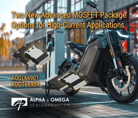
State-of-the-art topside cooling (GTPAK™) and gull-wing (GLPAK™) packages meet increased performance and robust environmental demands (Graphic: Business Wire)
The GTPAK offered with the AOGT66909 is a topside cooling package designed with a large exposed pad for more efficient heat transfer. The topside cooling technology transfers most heat to the heat sink mounted on the top exposed pad. This feature allows the GTPAK to offer a more effective thermal dissipation route than going through the PCB board, allowing a lower-cost PCB, such as FR4, to be used.
The GLPAK offered with the AOGL66901 is a gull-wing version of AOS’ successful TOLL package. It is designed using AOS’ advanced clip technology to achieve a high inrush current rating. The GLPAK with clip technology offers very low package resistance and parasitic inductance, improving EMI performance compared to other package types that employ standard wire bonding.
The GTPAK and GLPAK packages feature gull-wing leads, enabling excellent solder joint reliability even for insulated metal substrates (IMS) applications. This gull-wing construction also provides enhanced thermal cycling for IMS boards and other critical applications that must meet higher reliability objectives. AOS MOSFETs in the new GTPAK and GLPAK packages are manufactured in IATF16949-certified facilities and are compatible with automated optical inspection (AOI) manufacturing requirements.
“We are committed to delivering new solutions to help our customers meet or exceed their power performance requirements. By offering our industry-leading MOSFETs in the new robust GTPAK and GLPAK packages, AOS allows designers to select from two state-of-the-art packaging technologies that offer significant performance improvements. Furthermore, the advanced technologies in our AOGT66909 and AOGL66901 MOSFETs will help simplify new designs by reducing the number of devices needed while also providing the necessary higher current capability that makes overall system cost savings possible,” said Peter H. Wilson, Marketing Sr. Director of MOSFET product line at AOS.
Technical Highlights |
||||||||
|
||||||||
Part Number |
Package |
VDS (V) |
VGS (±V) |
TJ (°C) |
Continuous Drain Current (A) |
Pulsed Drain Current (A) |
RDS(ON) Max (mOhms) @10V |
|
@25°C |
@100°C |
@25°C |
||||||
GTPAK |
100 |
20 |
175 |
366 |
258 |
1464 |
1.5 |
|
GLPAK |
100 |
20 |
175 |
448 |
316 |
1790 |
1.25 |
|
Pricing and Availability
The AOGT66909 and AOGL66901 MOSFETs are immediately available in production quantities with a lead time of 14-16 weeks. The unit prices in 1,000-piece quantities are
About AOS
Alpha and Omega Semiconductor Limited, or AOS, is a designer, developer, and global supplier of a broad range of discrete power devices, wide bandgap power devices, power management ICs, and modules, including a wide portfolio of Power MOSFET, SiC, IGBT, IPM, TVS, HV Gate Drivers, Power IC, and Digital Power products. AOS has developed extensive intellectual property and technical knowledge that encompasses the latest advancements in the power semiconductor industry, which enables us to introduce innovative products to address the increasingly complex power requirements of advanced electronics. AOS differentiates itself by integrating its Discrete and IC semiconductor process technology, product design, and advanced packaging know-how to develop high-performance power management solutions. AOS’ portfolio of products targets high-volume applications, including personal computers, graphics cards, datacenters, AI servers, smartphones, consumer and industrial motor controls, TVs, lightings, automotive electronics, and power supply units for various equipment. For more information, please visit www.aosmd.com.
Forward-Looking Statements
This press release contains forward-looking statements based on current expectations, estimates, forecasts, and projections of future performance based on management’s judgment, beliefs, current trends, and anticipated product performance. These forward-looking statements include, without limitation, references to the efficiency and capability of new products and the potential to expand into new markets. Forward-looking statements involve risks and uncertainties that may cause actual results to differ materially from those in forward-looking statements. These factors include but are not limited to, the actual product performance in volume production, the quality and reliability of the product, our ability to achieve design wins, the general business and economic conditions, the state of the semiconductor industry, and other risks as described in the Company’s annual report and other filings with the
View source version on businesswire.com: https://www.businesswire.com/news/home/20250312879732/en/
Media Contact: Mina Galvan
Tel: 408.789.3233
Email: mina.galvan@aosmd.com
Source: Alpha and Omega Semiconductor Limited