SK hynix Develops Industry's First 12-Layer HBM3, Provides Samples To Customers
Rhea-AI Summary
SK hynix has developed the industry's first 12-layer HBM3 product with a remarkable 24GB memory capacity, marking a 50% increase from its previous 16GB model. Currently, customer performance evaluations are ongoing, with plans for mass production preparation to be finalized by the first half of 2023. The new product aims to meet rising demand for high-performance memory driven by the AI sector. Utilizing advanced MR-MUF and TSV technologies, this innovation enhances processing speeds up to 819GB per second. The adoption of HBM3 is expected to increase among major global tech companies, solidifying SK hynix's leadership in the cutting-edge DRAM market.
Positive
- Developed the industry's first 12-layer HBM3 product with a 24GB memory capacity.
- Increased memory capacity by 50% compared to previous 16GB model.
- Plans to commence mass production in the first half of 2023.
- Utilizes advanced technologies improving process efficiency and performance stability.
- Anticipated demand growth driven by the AI-powered chatbot industry.
Negative
- None.
News Market Reaction – HXSCL
On the day this news was published, HXSCL declined NaN%, reflecting a moderate negative market reaction.
Data tracked by StockTitan Argus on the day of publication.
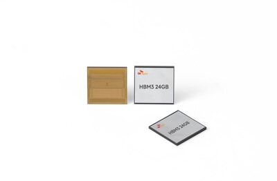
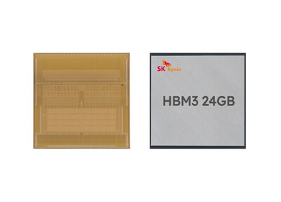
- Develops HBM3 product with industry's largest 24GB memory capacity; customers' performance evaluation of samples underway
- Features high-capacity and high-performance through stacking of 12 DRAM chips
- Plans to complete preparation for mass production by first half of 2023, aimed at solidifying company's leadership in cutting-edge DRAM market
* HBM (High Bandwidth Memory): A high-value, high-performance memory that vertically interconnects multiple DRAM chips and dramatically increases data processing speed in comparison to traditional DRAM products. HBM3 is the 4th generation product, succeeding the previous generations HBM, HBM2 and HBM2E
** Maximum memory capacity of the previously developed 8-layer HBM3 product was 16GB
"The company succeeded in developing the 24GB package product that increased the memory capacity by
SK hynix engineers improved process efficiency and performance stability by applying Advanced Mass Reflow Molded Underfill (MR-MUF)* technology to the latest product, while Through Silicon Via (TSV)** technology reduced the thickness of a single DRAM chip by
* MR-MUF (Mass Reflow Molded Underfill): A method of placing multiple chips on the lower substrate and bonding them at once through reflow, and then simultaneously filling the gap between the chips or between the chip and the substrate with a mold material.
** TSV (Through Silicon Via): An interconnecting technology used in advanced packaging that links the upper and lower chips with electrode that vertically passes through thousands of fine holes on DRAM chips. SK hynix's HBM3 that integrated this technology can process up to 819GB per second, meaning that 163 FHD (Full-HD) movies can be transmitted in a single second
The HBM, first developed by SK hynix in 2013, has drawn broad attention from the memory chip industry for its crucial role in implementing generative AI that operates in high-performance computing (HPC) systems.
The latest HBM3 standard, in particular, is considered the optimal product for rapid processing of large volumes of data, and therefore its adoption by major global tech companies is on the rise.
SK hynix has provided samples of its 24GB HBM3 product to multiple customers that have expressed great expectation for the latest product, while the performance evaluation of the product is in progress.
"SK hynix was able to continuously develop a series of ultra-high speed and high capacity HBM products through its leading technologies used in the back-end process," said
About
Media Contact
Global Public Relations
Technical Leader
E-Mail: global_newsroom@skhynix.com
Technical Leader
E-Mail: global_newsroom@skhynix.com
![]() View original content to download multimedia:https://www.prnewswire.com/news-releases/sk-hynix-develops-industrys-first-12-layer-hbm3-provides-samples-to-customers-301801630.html
View original content to download multimedia:https://www.prnewswire.com/news-releases/sk-hynix-develops-industrys-first-12-layer-hbm3-provides-samples-to-customers-301801630.html
SOURCE
FAQ
What is the significance of SK hynix's new 24GB HBM3 product?
When will SK hynix begin mass production of the 24GB HBM3?
What technologies did SK hynix use in the development of the 24GB HBM3?
How does the 24GB HBM3 benefit the AI industry?
What performance enhancements does the 24GB HBM3 offer compared to previous models?


