Synopsys Achieves Certification of its AI-driven Digital and Analog Flows and IP on Samsung Advanced SF2 GAA Process
Synopsys has announced that its AI-driven digital and analog design flows have achieved certification on Samsung Foundry's SF2 process with multiple test chip tapeouts. This certification validates the product readiness of its digital and analog design flows, enhanced by Synopsys.ai full-stack EDA suite, for Samsung's latest Gate-All-Around (GAA) process technologies. The optimized design flows offer significant improvements in performance, power, and area (PPA) with reported gains of 12% higher performance, 25% power reduction, and 5% area reduction.
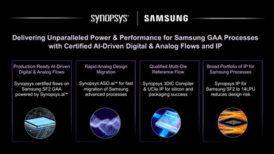
Additionally, the collaboration includes proven Synopsys IP on Samsung SF2, reducing integration risk and supporting 2.5D/3D heterogeneous integration. Synopsys' innovations in backside routing and nanosheet cell design further enhance the efficiency of designing for Samsung's GAA processes. The announcement also highlights the expanded Synopsys.ai collaboration, including Synopsys ASO.ai for faster analog design migration, and the availability of a multi-die design reference flow and UCIe IP for SF2.
- Certification of AI-driven digital and analog design flows on Samsung SF2 Process.
- Validated product readiness of certified flows with multiple test chip tapeouts.
- Performance improvements: 12% higher performance, 25% power reduction, 5% area reduction.
- Proven Synopsys IP reduces integration risk and accelerates silicon success.
- Qualified multi-die design reference flow and UCIe IP for SF2 process.
- Enhanced power distribution and efficiency with backside power and nanosheet optimization.
- Broadest portfolio of standards-compliant, silicon-proven interface IP.
- Accelerated design productivity and PPA optimization via Synopsys DSO.ai and ASO.ai.
- No specific negative aspects highlighted in the PR; however, reliance on new technology always carries inherent risk.
Insights
Synopsys' certification of its AI-driven digital and analog flows on Samsung's SF2 process is a game-changer in the semiconductor industry. This milestone underscores the power of AI in optimizing design processes, leading to superior performance, power efficiency and area (PPA) metrics. The successful tapeout of test chips indicates that the technology is production-ready, providing a reliable path for designers to meet aggressive timelines and performance goals.
The mention of a 12% increase in performance and a 25% reduction in power consumption is particularly noteworthy. These figures highlight the significant advantages of utilizing AI-driven design techniques compared to traditional methods. The integration of Synopsys' ASO.ai shows promise for faster analog design migration, which is critical as the industry moves towards more complex and heterogeneous designs. The introduction of new design techniques like backside routing and nanosheet cell design further positions Synopsys and Samsung at the forefront of innovation in the semiconductor space.
For retail investors, this development signifies Synopsys' strong foothold in the AI-driven EDA market and its ability to deliver cutting-edge technology that meets the evolving needs of high-performance computing and advanced packaging. However, it's essential to keep an eye on how these advancements translate into financial performance over the coming quarters.
The certification and multiple successful tapeouts on Samsung's SF2 process are a positive signal for Synopsys' business prospects. This achievement not only reinforces the company's technological leadership but also enhances its market position in the highly competitive EDA and IP sectors. The collaboration with a major foundry like Samsung could lead to increased revenue streams from licensing and design services, particularly as demand for custom SoCs and advanced packaging solutions grows.
From a financial perspective, the expected improvements in PPA (Performance, Power, Area) metrics could make Synopsys' solutions more attractive to a broader range of customers, thereby expanding its addressable market. The reduced integration risk and accelerated time to market afforded by Synopsys' certified flows and IP are likely to drive customer adoption, leading to potential revenue growth.
However, investors should also be mindful of the competitive landscape and the rapid pace of technological advancements in the semiconductor industry. Continuous innovation and maintaining strategic partnerships will be important for sustaining growth. Monitoring upcoming earnings reports and customer acquisition trends will provide further insights into the financial impact of these developments.
The announcement of Synopsys' certification on Samsung's SF2 process is significant, particularly in the context of the increasing demand for AI and high-performance computing (HPC) designs. The successful collaboration between Synopsys and Samsung indicates robust ecosystem support, which is critical for designers working on complex SoCs and multi-die integrations.
From a market perspective, Synopsys' advancements in AI-driven EDA tools and IP for advanced process nodes provide a competitive edge. The ability to deliver proven technology that enhances PPA metrics can be a compelling value proposition for customers in automotive, mobile and HPC segments. The broad portfolio of standards-compliant, silicon-proven interface IP further strengthens Synopsys' market position, enabling wide interoperability and reducing integration risks for customers.
Retail investors should consider the strategic implications of this development. Synopsys' continued innovation and partnership with Samsung are likely to drive market share gains and customer loyalty. The focus on next-generation processes like SF1.4 also indicates a forward-looking strategy, positioning the company well for future growth opportunities in the semiconductor industry.
Production-Ready Design Flows, Multi-Die Solution, and Synopsys IP Deliver a Proven Path to Unparalleled Power and Performance for AI and HPC Designs
Highlights
- Test chip tapeouts validate product readiness of certified digital and analog design flows for Samsung Foundry SF2/SF2Z process
- Collaboration on design techniques for SF2, including backside power and nanosheet optimization delivers more efficient power distribution
- Synopsys IP, now available and silicon proven on Samsung SF2, reduces integration risk and accelerates silicon success
- Qualified multi-die design reference flow and UCIe IP for SF2 process accelerates 2.5D/3D heterogeneous integration
- Expanded collaboration on Synopsys.ai includes Synopsys ASO.ai for accelerated analog design migration with new analog design migration reference flow for Samsung's GAA processes
"The demand for custom SoCs in the era of pervasive intelligence requires extensive ecosystem collaboration to help customers accelerate their innovation and silicon success on Samsung's SF2 and next-generation SF1.4 processes," said Sanjay Bali, vice president of product management and strategy for the EDA Group at Synopsys. "Achieving certification and multiple successful tapeouts of our digital and analog flows, powered by Synopsys.ai, on the SF2 process, combined with proven Synopsys IP provides designers with a trusted path to meeting their aggressive design goals for a faster time to market."
"Synopsys and Samsung have worked closely for decades to help our mutual customers achieve their most complex design requirements," said Sangyun Kim, Vice President and head of Foundry Design Technology Team at Samsung Electronics. "This latest collaboration milestone with Synopsys on AI-driven EDA flows and broad IP portfolio development is a testament to our ongoing efforts to address the industry's growing demand for high performance computing with significant PPA gains. Working together we validated our PPA results using Synopsys' certified digital flow, achieving
Collaboration on AI-driven EDA Flows
Synopsys and Samsung are closely collaborating on AI-driven flows, including Synopsys DSO.ai™ for design productivity and PPA optimization, and Synopsys ASO.ai™ for faster analog design migration. This collaboration has resulted in a new analog design migration reference flow using Synopsys ASO.ai for Samsung's FinFET to GAA processes, enabling designers to efficiently migrate Samsung 8nm analog IPs to SF2 process, adding to Synopsys' established flows on Samsung's 14nm to 8nm/SF5 processes.
New Design Techniques and Methodology for Advanced GAA Processes
Synopsys' continued innovation helps mutual customers benefit from new design techniques including backside routing, local layout effect-aware methodology, and nanosheet cell design, to help customers meet their design goals for power, performance, and area on Samsung SF2 process family. In addition, integrating backside routing and the super-cell approach using Synopsys' digital implementation and signoff tools enables designers to increase transistor performance efficiency and density, optimize power consumption, and reduce area by up to
Accelerate SoC and Multi-Die Designs
Synopsys IP for Samsung standard and automotive processes from SF2 to SF14LPU delivers a competitive edge for chipmakers looking to reduce integration risk and accelerate time to silicon success for automotive, mobile, high-performance computing (HPC) and multi-die designs. The industry's broadest portfolio of standards-compliant, silicon-proven interface IP for advanced Samsung processes, including PCIe 6.0/5.0/4.0, DDR5, LPDDR5X/5/4X, MIPI M-PHY G5, eUSB2, USB 3.2/3.1, and DisplayPort enables wide interoperability for commonly used protocols. To accelerate integration of chiplets in multi-die packages, Synopsys UCIe IP has taped out in SF2 and SF4x, and achieved silicon success in SF5A process technologies, to deliver robust die-to-die connectivity with low power and low latency. Synopsys Foundation IP, including embedded memories, logic libraries and GPIOs, is also proven in silicon to deliver leading power, performance, and area in a range of Samsung process technologies.
Mutual customers can accelerate the development of multi-die designs using Synopsys 3DIC Compiler, a unified exploration-to-signoff platform for 2.5D and 3D heterogeneous integration and advanced packaging. Qualified for Samsung Foundry's SF2 process, Synopsys 3DIC Compiler supports Samsung's advanced silicon processes, packaging technologies, and 3DCODE standard. Synopsys is an active member of the Samsung Foundries' MDI Alliance, helping mutual customers achieve a successful transition to 2.5D and 3D advanced packaging designs.
About Synopsys
Catalyzing the era of pervasive intelligence, Synopsys, Inc. (Nasdaq: SNPS) delivers trusted and comprehensive silicon to systems design solutions, from electronic design automation to silicon IP and system verification and validation. We partner closely with semiconductor and systems customers across a wide range of industries to maximize their R&D capability and productivity, powering innovation today that ignites the ingenuity of tomorrow. Learn more at www.synopsys.com.
Editorial Contact
Kelli Wheeler
Synopsys, Inc.
(650) 584-5000
kelliw@synopsys.com
corp-pr@synopsys.com
![]() View original content to download multimedia:https://www.prnewswire.com/news-releases/synopsys-achieves-certification-of-its-ai-driven-digital-and-analog-flows-and-ip-on-samsung-advanced-sf2-gaa-process-302171192.html
View original content to download multimedia:https://www.prnewswire.com/news-releases/synopsys-achieves-certification-of-its-ai-driven-digital-and-analog-flows-and-ip-on-samsung-advanced-sf2-gaa-process-302171192.html
SOURCE Synopsys, Inc.


