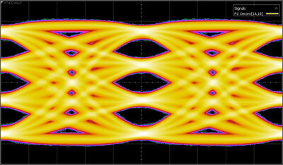
Marvell Demonstrates Industry's First 3nm Data Infrastructure Silicon
Marvell Technology (NASDAQ: MRVL) has unveiled its industry-first silicon building blocks created on TSMC's 3-nanometer (3nm) process. This includes high-speed SerDes and innovative die-to-die interconnects designed to enhance data infrastructure performance. These new technologies enable data transfer rates up to 240 Tbps, which is 45% faster than current multichip packaging alternatives, significantly reducing system-level bottlenecks. Marvell's advancements support various sectors including cloud computing, AI, and 5G. The company continues to build on its strong portfolio of silicon IP, pushing the boundaries for chips that demand high bandwidth and energy efficiency. With these improvements, Marvell aims to meet the increasing data demands of modern computing systems, particularly in hyperscale data centers.
- Industry-first 3nm silicon building blocks.
- Achieves data transfer rates up to 240 Tbps.
- 45% faster than existing multichip packaging options.
- Enhances performance across cloud, AI, and networking solutions.
- Continues to lead in silicon IP for advanced semiconductor designs.
- None.
Insights
Analyzing...
- The 3nm building blocks include high-speed SerDes and parallel interconnects for dramatically boosting the performance of next-generation data infrastructure
- Innovative die-to-die interconnects will enable data transfer speeds at up to 240 Tbps,
45% faster than available alternatives in multichip packages - Extends Marvell's silicon IP leadership for cloud, AI, networking, 5G, automotive and custom solutions
SANTA CLARA, Calif., April 19, 2023 /PRNewswire/ -- Marvell Technology, Inc. (NASDAQ: MRVL), a leader in data infrastructure semiconductor solutions, has demonstrated high-speed, ultra-high bandwidth silicon interconnects produced on Taiwan Semiconductor Manufacturing Company's (TSMC) 3-nanometer (3nm) process. Marvell's industry-first silicon building blocks in this node include 112G XSR SerDes (serializer/de-serializer), Long Reach SerDes, PCIe Gen 6 / CXL 3.0 SerDes, and a 240 Tbps parallel die-to-die interconnect.
The new building blocks are part of Marvell's continued execution of its strategy to develop a comprehensive silicon IP portfolio for designing chips that will radically increase the bandwidth, performance, and energy efficiency of next-generation data infrastructure. These technologies also support all semiconductor packaging options from standard and low-cost RDL (Redistribution Layers) to silicon-based high-density interconnect.
Marvell was also the first data infrastructure silicon supplier to respectively sample and commercially release the industry-leading 112G SerDes and has been a leader in data infrastructure products based on TSMC's 5nm process.
SerDes and parallel interconnects serve as high-speed pathways for exchanging data between chips or silicon components inside chiplets. Together with 2.5D and 3D packaging, these technologies will eliminate system-level bottlenecks to advance the most complex semiconductor designs. SerDes also help reduce pins, traces and circuit board space to reduce cost. A rack in a hyperscale data center might contain tens of thousands of SerDes links.
The new parallel die-to-die interconnect, for example, enables aggregate data transfers up to 240 Tbps,
Marvell incorporates its SerDes and interconnect technologies into its flagship silicon solutions including Teralynx® switches, PAM4 and coherent DSPs, Alaska® Ethernet physical layer (PHY) devices, OCTEON® processors, Bravera™ storage controllers, Brightlane™ automotive Ethernet chipsets, and custom ASICs. Moving to a 3nm process enables engineers to lower the cost and power consumption of chips and computing systems while maintaining signal integrity and performance.
"Interconnects are taking on heightened importance as clouds and other computing systems grow in size, complexity and capability. Our advanced SerDes and parallel interfaces will play a significant role in providing a platform for developing chips with best-in-class bandwidth, latency, bit error rate, and power efficiency for meeting the demands of AI and other complex workloads," said Raghib Hussain, president of products and technologies at Marvell. "We are proud to be able to deliver such advances on TSMC's 3nm technology and take semiconductor designs to the next level for our customers around the world."
"Bandwidth is the lifeblood of the cloud. Service providers are growing their network capacity by approximately
"We congratulate Marvell on the achievement of this important silicon development milestone in the industry's cutting-edge 3nm process technology," said Joachim Peerlings, general manager of Keysight's Communications Solutions Group. "We are very pleased with our progress on the broader industry enablement and excited to work with top technology innovators like Marvell to showcase next generation interconnect technologies that will help push the boundaries of data infrastructure silicon design, performance and energy efficiency."
About Marvell
To deliver the data infrastructure technology that connects the world, we're building solutions on the most powerful foundation: our partnerships with our customers. Trusted by the world's leading technology companies for over 25 years, we move, store, process and secure the world's data with semiconductor solutions designed for our customers' current needs and future ambitions. Through a process of deep collaboration and transparency, we're ultimately changing the way tomorrow's enterprise, cloud, automotive, and carrier architectures transform—for the better.
Marvell and the M logo are trademarks of Marvell or its affiliates. Please visit www.marvell.com for a complete list of Marvell trademarks. Other names and brands may be claimed as the property of others.
This press release contains forward-looking statements within the meaning of the federal securities laws that involve risks and uncertainties. Forward-looking statements include, without limitation, any statement that may predict, forecast, indicate or imply future events or achievements. Actual events or results may differ materially from those contemplated in this press release. Forward-looking statements speak only as of the date they are made. Readers are cautioned not to put undue reliance on forward-looking statements, and no person assumes any obligation to update or revise any such forward-looking statements, whether as a result of new information, future events or otherwise.
For further information, contact:
Michael Kanellos, Head of Influencer Relations
pr@marvell.com
![]() View original content to download multimedia:https://www.prnewswire.com/news-releases/marvell-demonstrates-industrys-first-3nm-data-infrastructure-silicon-301801383.html
View original content to download multimedia:https://www.prnewswire.com/news-releases/marvell-demonstrates-industrys-first-3nm-data-infrastructure-silicon-301801383.html
SOURCE Marvell


