Keysight Launches Comprehensive Solution for Accurate and Seamless Photonic Circuit Design
Keysight Technologies (NYSE: KEYS) has launched Photonic Designer, a new photonic design automation (PDA) software solution within its Advanced Design System (ADS) suite. This comprehensive tool addresses key challenges in photonic integrated circuit design by providing:
- A unified platform for seamless workflow from concept to manufacturing
- Physics-driven simulation environment for accurate performance prediction
- Direct integration of real-world measurement data
- Compatibility with foundry Process Design Kits (PDKs)
The software enables engineers to verify designs against industry standards pre-fabrication, optimize photonic models for foundry processes, and accelerate design verification. CompoundTek, a photonics foundry services provider, is offering a Photonic Designer PDK for Keysight ADS users, facilitating the development of PICs with foundry-verified components.
Keysight Technologies (NYSE: KEYS) ha lanciato Photonic Designer, una nuova soluzione software di automazione del design fotonico (PDA) all'interno della sua suite Advanced Design System (ADS). Questo strumento completo affronta le principali sfide nella progettazione di circuiti integrati fotonici fornendo:
- Una piattaforma unificata per un flusso di lavoro senza interruzioni dal concetto alla produzione
- Un ambiente di simulazione basato sulla fisica per previsioni di prestazioni accurate
- Integrazione diretta di dati di misurazione reali
- Compatibilità con i Process Design Kits (PDK) delle fonderie
Il software consente agli ingegneri di verificare i progetti rispetto agli standard industriali prima della fabbricazione, ottimizzare i modelli fotonici per i processi delle fonderie e accelerare la verifica del design. CompoundTek, un fornitore di servizi di fonderia fotonica, sta offrendo un PDK di Photonic Designer per gli utenti di Keysight ADS, facilitando lo sviluppo di PIC con componenti verificati dalla fonderia.
Keysight Technologies (NYSE: KEYS) ha lanzado Photonic Designer, una nueva solución de software de automatización de diseño fotónico (PDA) dentro de su suite Advanced Design System (ADS). Esta herramienta integral aborda los principales desafíos en el diseño de circuitos integrados fotónicos al proporcionar:
- Una plataforma unificada para un flujo de trabajo sin interrupciones desde el concepto hasta la fabricación
- Un entorno de simulación impulsado por la física para predicciones de rendimiento precisas
- Integración directa de datos de medición del mundo real
- Compatibilidad con los Process Design Kits (PDK) de las fundiciones
El software permite a los ingenieros verificar los diseños según los estándares de la industria antes de la fabricación, optimizar los modelos fotónicos para los procesos de fundición y acelerar la verificación del diseño. CompoundTek, un proveedor de servicios de fundición fotónica, está ofreciendo un PDK de Photonic Designer para los usuarios de Keysight ADS, facilitando el desarrollo de PIC con componentes verificados por la fundición.
Keysight Technologies (NYSE: KEYS)는 Photonic Designer를 출시했습니다. 이 새로운 포토닉 디자인 자동화(PDA) 소프트웨어 솔루션은 고급 디자인 시스템(ADS) 제품군의 일부입니다. 이 포괄적인 도구는 포토닉 집적 회로 설계에서의 주요 과제를 해결하기 위해 다음과 같은 기능을 제공합니다:
- 개념에서 제조까지 원활한 워크플로를 위한 통합 플랫폼
- 정확한 성능 예측을 위한 물리 기반 시뮬레이션 환경
- 실제 측정 데이터의 직접 통합
- 파운드리 프로세스 디자인 키트(PDK)와의 호환성
이 소프트웨어는 엔지니어가 제조 전에 산업 표준에 따라 설계를 검증하고, 파운드리 프로세스를 위한 포토닉 모델을 최적화하며, 설계 검증을 가속화할 수 있도록 합니다. 포토닉스 파운드리 서비스 제공업체인 CompoundTek은 Keysight ADS 사용자에게 Photonic Designer PDK를 제공하여 파운드리 검증된 구성 요소로 PIC 개발을 촉진하고 있습니다.
Keysight Technologies (NYSE: KEYS) a lancé Photonic Designer, une nouvelle solution logicielle d'automatisation de la conception photonique (PDA) au sein de sa suite Advanced Design System (ADS). Cet outil complet répond aux principaux défis de la conception de circuits intégrés photoniques en fournissant :
- Une plateforme unifiée pour un flux de travail sans couture, du concept à la fabrication
- Un environnement de simulation basé sur la physique pour des prévisions de performance précises
- Intégration directe des données de mesure du monde réel
- Compatibilité avec les kits de conception de processus (PDK) des fonderies
Le logiciel permet aux ingénieurs de vérifier les conceptions par rapport aux normes de l'industrie avant la fabrication, d'optimiser les modèles photoniques pour les processus de fonderie et d'accélérer la vérification de la conception. CompoundTek, un fournisseur de services de fonderie photonique, propose un PDK de Photonic Designer pour les utilisateurs de Keysight ADS, facilitant le développement de PIC avec des composants vérifiés par la fonderie.
Keysight Technologies (NYSE: KEYS) hat Photonic Designer eingeführt, eine neue Softwarelösung zur Automatisierung des photonischen Designs (PDA) innerhalb seiner Advanced Design System (ADS) Suite. Dieses umfassende Werkzeug adressiert die wichtigsten Herausforderungen im Design von photonischen integrierten Schaltungen, indem es Folgendes bereitstellt:
- Eine einheitliche Plattform für einen nahtlosen Workflow vom Konzept bis zur Fertigung
- Eine physikbasierte Simulationsumgebung für präzise Leistungsprognosen
- Direkte Integration von realen Messdaten
- Kompatibilität mit den Process Design Kits (PDK) der Foundries
Die Software ermöglicht es Ingenieuren, Designs vor der Fertigung an Industriestandards zu überprüfen, photonische Modelle für Foundry-Prozesse zu optimieren und die Designverifizierung zu beschleunigen. CompoundTek, ein Anbieter von Photonik-Fundierungsdiensten, bietet ein Photonic Designer PDK für Keysight ADS-Nutzer an, um die Entwicklung von PICs mit von der Foundry verifizierten Komponenten zu erleichtern.
- Launch of new comprehensive software solution expanding product portfolio
- Strategic partnership with CompoundTek for PDK integration
- Product addresses efficiency gaps in current market solutions
- Potential for reduced time-to-market for customers
- None.
Insights
Keysight's launch of Photonic Designer represents a strategic expansion in the high-growth photonics design market. This software addresses critical industry pain points including fragmented workflows and simulation inconsistencies that currently plague photonic integrated circuit (PIC) designers.
The product strengthens Keysight's position in the electronic design automation (EDA) space by extending capabilities into photonics—a important technology for next-generation computing, telecommunications, and data transmission applications. By integrating this solution into their existing Advanced Design System suite, Keysight creates valuable cross-selling opportunities across their customer base.
Particularly significant is the collaboration with CompoundTek, which adds foundry verification to the offering. This partnership model could prove scalable if Keysight secures additional foundry relationships, potentially creating a network effect that increases the software's value proposition.
The timing aligns with growing industry demand for more efficient photonic design tools as companies seek to overcome limitations of traditional electronic circuits. While financial projections aren't provided, this launch represents Keysight executing on its core strategy of addressing high-value technical challenges with software-centric solutions that complement their test and measurement hardware portfolio.
Keysight's Photonic Designer addresses a significant technical gap in the photonic integrated circuit (PIC) development ecosystem. Current PIC designers typically juggle multiple disconnected tools across the design-to-manufacturing pipeline, creating inefficiencies and accuracy issues that this solution directly targets.
The physics-driven simulation approach is particularly valuable as it integrates real-world measurement data into workflows—a critical advancement for a field where theoretical models often diverge from manufacturing realities. This capability to verify designs against industry modulation standards before fabrication represents substantial time and cost savings potential.
CompoundTek's PDK integration is technically significant as it bridges the design-to-fabrication gap. Silicon photonics has faced adoption challenges partly due to the complexity of transitioning designs to manufacturing-ready specifications, and this collaboration demonstrates progress in standardizing these workflows.
Most impressive is the software's ability to handle combined electrical-optical-electrical workflows, recognizing that photonic systems rarely exist in isolation from electronics. This holistic approach positions the tool for applications in data centers, telecommunications, and quantum computing—all fields requiring integrated photonic-electronic solutions. The technical capabilities suggest Keysight is targeting the full spectrum of photonic design challenges rather than merely incremental improvements to existing processes.
- Optimizes photonic integrated circuit performance with advanced physics-based simulation
- Eliminates fragmented workflows and improves design accuracy with a holistic photonic design automation tool
- Ensures compliance and manufacturing readiness with process design kit customization and real-world data integration
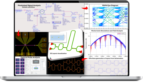
From concept to validation—Photonic Designer streamlines the entire photonic design process with a comprehensive automation solution.
Photonics design engineers often face challenges with scattered tool chains and simulation discrepancies that hinder efficiency and precision. Traditional workflows require engineers to switch between multiple software platforms, making it challenging to ensure design consistency. Keysight’s Photonic Designer, part of the Advanced Design System (ADS) suite of tools, eliminates these inefficiencies by offering a comprehensive, physics-driven simulation environment that accurately predicts real-world circuit performance. Keysight tools also support an open, interoperable workflow ecosystem for maximum flexibility.
Photonic Designer integrates real-world measurement data directly into the simulation workflow, to optimize models and streamline compliance and validation. This allows engineers to:
- Verify designs against industry modulation standards before fabrication.
- Use models with best-in-class simulators to ensure accurate, confident, robust designs.
- Ensure seamless compatibility with foundry PDKs to avoid costly iterations.
- Optimize photonic model variables to match foundry processes to align with manufacturing conditions.
- Automate and accelerate design verification, reducing go-to-market time.
The software is designed to streamline pure optical and combined electrical-optical-electrical workflows for circuit design, providing an intuitive interface for effortless circuit design and layout generation. Engineers can simulate, validate, and optimize photonic circuits while ensuring compliance with stringent design rules, guaranteeing precision and reliability.
To further enhance the design process, CompoundTek, a leading provider of photonics foundry services, is offering a Photonic Designer PDK for Keysight ADS users, for their silicon photonics process. This collaboration enables engineers to develop PICs with foundry-verified components, ensuring seamless transition from design to fabrication.
S. Gunasagar, Chief Operating Officer at CompoundTek said: “We are excited to offer a highly accurate PDK for our silicon photonics process. This integration with Keysight’s ADS allows engineers to confidently design and validate photonic circuits with the assurance of manufacturing compatibility, ultimately accelerating time-to-market for innovative solutions.”
Nilesh Kamdar, EDA Design & Verification General Manager at Keysight, said: “Engineers need a reliable and precise environment to design and validate photonic integrated circuits without unnecessary tool-switching. Photonic Designer provides a single, unified platform that integrates physics-based simulations, PDK customization, and compliance verification, ensuring high-fidelity results from concept to manufacturing.”
Resources
- Application Note: Optimizing Photodetector Model to a Silicon Photonics Foundry Process
- Product Page: Photonic Designer
- Video: Photonic Designer
- Video: How to use the Optical Mode Solver from Keysight Photonic Designer
More Information: Attend the Keysight Booth at OFC 2025
Visit the Keysight booth #1301 at the OFC 2025 conference to learn more about Photonic Designer and its capabilities.
About Keysight Technologies
At Keysight (NYSE: KEYS), we inspire and empower innovators to bring world-changing technologies to life. As an S&P 500 company, we’re delivering market-leading design, emulation, and test solutions to help engineers develop and deploy faster, with less risk, throughout the entire product life cycle. We’re a global innovation partner enabling customers in communications, industrial automation, aerospace and defense, automotive, semiconductor, and general electronics markets to accelerate innovation to connect and secure the world. Learn more at Keysight Newsroom and www.keysight.com.
View source version on businesswire.com: https://www.businesswire.com/news/home/20250319611958/en/
Keysight Media Contacts
North America PR Team
pdl-americas-keysight@keysight.com
Fusako Dohi
+81 42 660-2162
fusako_dohi@keysight.com
Jenny Gallacher
+44 118 927 4003
jenny.gallacher@keysight.com
Source: Keysight Technologies, Inc.