Keysight Expands Chiplet Interconnect Standards Support in Chiplet PHY Designer 2025
Keysight Technologies (NYSE: KEYS) has announced the launch of Chiplet PHY Designer 2025, an enhanced software solution for high-speed digital chiplet design focused on AI and data center applications. The new version introduces support for the Universal Chiplet Interconnect Express™ (UCIe™) 2.0 standard and adds compatibility with the Open Computer Project Bunch of Wires (BoW) standard.
The solution enables pre-silicon level validation and streamlines the path to tapeout. Key benefits include ensuring interoperability across advanced packaging ecosystems, accelerating time-to-market through automated simulation and compliance testing, improving design accuracy through signal integrity analysis, and optimizing clocking designs with quarter-rate data rate support.
Keysight will showcase the Chiplet PHY Designer at DesignCon booth #1039 at the Santa Clara Convention Center from January 29-30, 2025.
Keysight Technologies (NYSE: KEYS) ha annunciato il lancio di Chiplet PHY Designer 2025, una soluzione software avanzata per la progettazione di chiplet digitali ad alta velocità, focalizzata su applicazioni di intelligenza artificiale e centri dati. La nuova versione introduce il supporto per lo standard Universal Chiplet Interconnect Express™ (UCIe™) 2.0 e aggiunge compatibilità con lo standard Open Computer Project Bunch of Wires (BoW).
La soluzione consente validazioni a livello pre-silicio e semplifica il percorso verso il tapeout. I principali vantaggi includono la garanzia di interoperabilità tra ecosistemi di imballaggio avanzati, l'accelerazione del time-to-market attraverso simulazioni automatizzate e test di conformità, il miglioramento della precisione progettuale attraverso analisi dell'integrità del segnale e l'ottimizzazione dei design di clock con supporto per una velocità di dati a un quarto di rate.
Keysight presenterà il Chiplet PHY Designer presso il DesignCon, stand #1039, al Centro Congressi di Santa Clara dal 29 al 30 gennaio 2025.
Keysight Technologies (NYSE: KEYS) ha anunciado el lanzamiento de Chiplet PHY Designer 2025, una solución de software mejorada para el diseño de chiplets digitales de alta velocidad centrada en aplicaciones de inteligencia artificial y centros de datos. La nueva versión introduce soporte para el estándar Universal Chiplet Interconnect Express™ (UCIe™) 2.0 y añade compatibilidad con el estándar Open Computer Project Bunch of Wires (BoW).
La solución permite la validación a nivel pre-silicio y agiliza el camino hacia el tapeout. Los principales beneficios incluyen asegurar la interoperabilidad entre ecosistemas de empaquetado avanzados, acelerar el tiempo de comercialización mediante simulaciones automatizadas y pruebas de conformidad, mejorar la precisión del diseño a través del análisis de la integridad de la señal y optimizar los diseños de reloj con soporte para tasas de datos a un cuarto.
Keysight mostrará el Chiplet PHY Designer en DesignCon, booth #1039, en el Centro de Convenciones de Santa Clara del 29 al 30 de enero de 2025.
Keysight Technologies (NYSE: KEYS)는 AI 및 데이터 센터 애플리케이션에 중점을 둔 고속 디지털 칩렛 설계를 위한 향상된 소프트웨어 솔루션인 Chiplet PHY Designer 2025의 출시를 발표했습니다. 새 버전은 Universal Chiplet Interconnect Express™ (UCIe™) 2.0 표준을 지원하며, Open Computer Project Bunch of Wires (BoW) 표준과의 호환성을 추가합니다.
이 솔루션은 실리콘 제작 전 단계에서의 검증을 가능하게 하고, 테이프 아웃으로 가는 경로를 간소화합니다. 주요 이점에는 고급 패키징 생태계 전반에 걸쳐 상호 운용성 보장, 자동화된 시뮬레이션 및 규정 준수 테스트를 통한 시장 출시 시간 단축, 신호 무결성 분석을 통한 설계 정확성 향상, 분기 속도 지원을 통한 클록 설계 최적화가 포함됩니다.
Keysight는 2025년 1월 29일부터 30일까지 샌타클라라 컨벤션 센터에서 열리는 DesignCon에서 Chiplet PHY Designer를 전시할 예정입니다. 부스 번호는 #1039입니다.
Keysight Technologies (NYSE: KEYS) a annoncé le lancement de Chiplet PHY Designer 2025, une solution logicielle améliorée pour la conception de chiplets numériques à haut débit axée sur les applications d'IA et les centres de données. La nouvelle version introduit le support du standard Universal Chiplet Interconnect Express™ (UCIe™) 2.0 et ajoute la compatibilité avec le standard Open Computer Project Bunch of Wires (BoW).
Cette solution permet une validation au niveau pré-silicon et simplifie le chemin vers le tapeout. Les principaux avantages incluent la garantie d'interopérabilité entre des écosystèmes d'emballage avancés, l'accélération du temps de mise sur le marché grâce à des simulations automatisées et des tests de conformité, l'amélioration de la précision de conception grâce à l'analyse de l'intégrité du signal, et l'optimisation des conceptions d'horloge avec support pour des taux de données à un quart.
Keysight présentera le Chiplet PHY Designer lors de DesignCon au stand #1039 au Centre de Convention de Santa Clara du 29 au 30 janvier 2025.
Keysight Technologies (NYSE: KEYS) hat die Einführung des Chiplet PHY Designer 2025 angekündigt, einer verbesserten Softwarelösung für das Design von Hochgeschwindigkeits-Digitalchiplets, die auf KI- und Rechenzentrumsanwendungen fokussiert ist. Die neue Version führt die Unterstützung für den Standard Universal Chiplet Interconnect Express™ (UCIe™) 2.0 ein und ergänzt die Kompatibilität mit dem Standard Open Computer Project Bunch of Wires (BoW).
Die Lösung ermöglicht die Validierung auf der Pre-Silicon-Ebene und vereinfacht den Weg bis zum Tapeout. Zu den wichtigsten Vorteilen gehören die Gewährleistung der Interoperabilität zwischen fortschrittlichen Verpackungsökosystemen, die Verkürzung der Markteinführungszeit durch automatisierte Simulationen und Konformitätstests, die Verbesserung der Entwurfsgenauigkeit durch Signalintegritätsanalysen sowie die Optimierung von Taktentwürfen mit Unterstützung für Datenraten im Viertel-Takt.
Keysight wird den Chiplet PHY Designer auf der DesignCon am Stand #1039 im Santa Clara Convention Center vom 29. bis 30. Januar 2025 präsentieren.
- Introduction of new standards support (UCIe 2.0 and BoW) enhances product capabilities
- Automated simulation and compliance testing features reduce time-to-market
- Pre-silicon validation capabilities reduce costly silicon re-spins
- None.
Insights
The launch of Chiplet PHY Designer 2025 with UCIe 2.0 and BoW standards support represents a strategic advancement in Keysight's EDA portfolio. In the current semiconductor landscape, where chiplet design is becoming increasingly critical for AI and data center applications, this tool addresses a important market need. The introduction of quarter-rate data rate (QDR) analysis capabilities and systematic crosstalk analysis for single-ended buses significantly enhances the solution's value proposition.
Think of chiplets as LEGO blocks in semiconductor design - they need to fit and work together perfectly. This software acts like a digital testing ground, ensuring these blocks will connect and communicate flawlessly before expensive manufacturing begins. The pre-silicon validation capabilities could potentially reduce development costs by millions of dollars by catching issues before tape-out, where fixes become exponentially more expensive.
The timing of this release aligns perfectly with the industry's shift toward disaggregated chip design, particularly as companies seek more cost-effective solutions for complex AI and data center chips. The inclusion of UCIe 2.0 support is particularly noteworthy as this standard is gaining significant industry traction, with major players like Intel, TSMC and AMD adopting it.
This product launch strengthens Keysight's position in the rapidly growing chiplet design software market. With the global chiplet market projected to reach
For investors, this represents Keysight's strong execution in high-growth segments of the semiconductor industry. The company's focus on AI and data center applications - two of the fastest-growing sectors in technology - positions it well for sustained growth. The endorsement from Alphawave Semi, a notable player in high-speed connectivity, adds credibility to the solution's capabilities and market potential.
- Introduces support for the latest interconnect standards, including Universal Chiplet Interconnect Express™ (UCIe™) 2.0 and Open Compute Project Bunch of Wires (BoW).
- Enhances Keysight’s EDA standards-based approach, enabling high-speed digital chiplet design tailored for AI and data center applications.

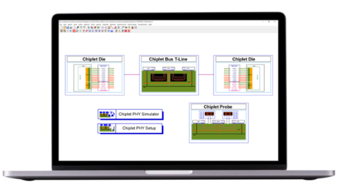
Chiplet PHY Designer provides engineers with an intuitive and integrated chiplet system analysis environment. (Photo: Business Wire)
As AI and data center chips grow more complex, ensuring reliable communication between chiplets becomes crucial for performance. The industry is addressing this challenge through open, emerging standards like UCIe and BoW that define the interconnects between chiplets within an advanced 2.5D/3D package. By adopting these standards and verifying chiplets for compliance, designers contribute to the growing ecosystem for chiplet interoperability, reducing costs and risks in semiconductor development.
Key Benefits of the Chiplet PHY Designer 2025:
- Ensures Interoperability: Verifies designs meet UCIe 2.0 and BoW standards, enabling seamless integration across advanced packaging ecosystems.
- Accelerates Time-to-Market: Automates simulation and compliance testing setup, such as Voltage Transfer Function (VTF), simplifying chiplet design workflows.
- Improves Design Accuracy: Provides insight into signal integrity, bit error rate (BER), and crosstalk analysis, reducing risks of costly silicon re-spins.
- Optimizes Clocking Designs: Supports advanced clocking scheme analysis, such as quarter-rate data rate (QDR), for precise synchronization in high-speed interconnects.
Hee-Soo Lee, High-Speed Digital Segment Lead, Keysight EDA, said: “Keysight EDA launched Chiplet PHY Designer one year ago as the industry’s first pre-silicon validation tool to provide in-depth modeling and simulation capabilities; this enabled chiplet designers to rapidly and accurately verify that their designs meet specifications before tapeout. The latest release keeps pace with evolving standards like UCIe 2.0 and BoW while delivering new features, such as the QDR clocking scheme and systematic crosstalk analysis for single-ended buses. Engineers using Chiplet PHY Designer save time and avoid costly rework, ensuring their designs meet performance requirements before manufacturing. Early adopters, like Alphawave Semi, attest that Chiplet PHY Designer ensures seamless operation and interoperability for 2.5D/3D solutions available to their chiplet customers.”
See Chiplet PHY Designer at DesignCon
Keysight will demonstrate Chiplet PHY Designer at its DesignCon booth, #1039, at the
Resources:
About Keysight Technologies
At Keysight (NYSE: KEYS), we inspire and empower innovators to bring world-changing technologies to life. As an S&P 500 company, we’re delivering market-leading design, emulation, and test solutions to help engineers develop and deploy faster, with less risk, throughout the entire product life cycle. We’re a global innovation partner enabling customers in communications, industrial automation, aerospace and defense, automotive, semiconductor, and general electronics markets to accelerate innovation to connect and secure the world. Learn more at Keysight Newsroom and www.keysight.com.
View source version on businesswire.com: https://www.businesswire.com/news/home/20250121466743/en/
Keysight Media Contacts
North America PR Team
pdl-americas-keysight-pr@keysight.com
Fusako Dohi
+81 42 660-2162
fusako_dohi@keysight.com
Jenny Gallacher
+44 (0) 7800 737 982
jenny.gallacher@keysight.com
Source: Keysight Technologies, Inc.


