CyberOptics to Showcase High-Precision Inspection and Metrology Solutions at the SEMI Connecting Heterogeneous Systems Summit
CyberOptics Corporation (NASDAQ: CYBE) showcased its WX3000™ metrology system featuring MRS™ sensor technology at the Virtual Connecting Heterogeneous Systems Summit. The event, held from Sept. 1-3, 2021, includes a presentation by VP Tim Skunes on improving plating uniformity in hybrid bonding. The WX3000™ offers sub-micrometer accuracy for wafer inspections, with throughput exceeding 25 wafers per hour. The company emphasizes the importance of fast, accurate metrology for advanced packaging applications, aiming to enhance yields and processes significantly.
- Showcasing WX3000™ metrology system with advanced MRS™ sensor technology enhances competitive positioning.
- Demonstrations at the summit could lead to increased sales opportunities in semiconductor markets.
- Fast, accurate inspection capabilities could significantly improve customers' yields and processes.
- Potential risks from market conditions and trade relations may impact future revenue.
- Dependence on foreign customers exposes the company to geopolitical risks.
- Ongoing price competition may pressure margins on product sales.
Insights
Analyzing...
CyberOptics® Corporation (NASDAQ: CYBE), a leading global developer and manufacturer of high-precision 3D sensing technology solutions, will feature the WX3000™ metrology and inspection system with MRS™ sensor technology, and high-precision sensors for semiconductor tool set-up and diagnostics at the Virtual Connecting Heterogeneous Systems Summit Sept. 1-3, 2021.

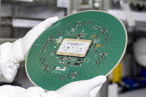
WaferSense Auto Resistance Sensor (ARS) (Photo: Business Wire)
Tim Skunes, CyberOptics VP of R&D, will share a presentation ‘Improving Plating Uniformity for Hybrid Bonding and Micro Bumping,’ on Sept. 2nd at 8:50 a.m. ET/2:50 p.m. European CT.
Recent results have correlated copper thickness variations across a wafer during electrochemical deposition (ECD) to variations in metal dishing depth variations in hybrid bonding applications. Copper pillar coplanarity is also correlated to ECD plating uniformity in wafer bumping applications. The plating uniformity during ECD is directly affected by plating cell contact resistance. In-process monitoring of plating cell contact resistance can accurately predict when preventive maintenance is required to maintain thickness uniformity and save time and costs associated with test wafer measurements. A real-time sensor for measuring plating cell contact resistance will be presented.
The company will virtually demonstrate high-precision sensors that process and equipment engineers use in the front-end of the fab to speed equipment qualification, shorten equipment maintenance cycles, lower equipment expenses and optimize preventative maintenance plans. The WaferSense® Auto Resistance Sensor™ (ARS) enables real-time resistance measurements of plating cell contacts in semiconductor ECD applications.
The company also will virtually showcase the 3µm NanoResolution Multi-Reflection Suppression™ (MRS™) sensor integrated into CyberOptics’ WX3000™ system that provides sub-micrometer accuracy on features as small as 25µm. While retaining its ability to reject spurious multiple reflections, it adds the ability to capture and analyze specular reflections from shiny surfaces of solder balls, bumps and pillars, allowing highly accurate inspection and 3D metrology of these critical packaging features. Fast, complete
“Fast, 100 percent metrology and inspection is needed now more than ever for wafer-level and advanced packaging applications,” said Dr. Subodh Kulkarni, President and CEO, CyberOptics. “Compared to alternative technologies, our systems are 2-3X faster with the high resolution and accuracy required to enable our customers to recognize significant improvements in yields and processes.”
The SEMI Connected Heterogeneous Systems Summit brings together thought leaders and industry experts from the entire 3D & Systems and packaging and, MEMS/imaging/sensor value chain to discuss the latest advancements in Heterogeneous Integration and sensing technology driving innovation in high end applications. CyberOptics is a gold sponsor.
For more information, visit www.cyberoptics.com.
About CyberOptics
CyberOptics Corporation (www.cyberoptics.com) is a leading global developer and manufacturer of high-precision 3D sensing technology solutions. CyberOptics’ sensors are used for inspection and metrology in the SMT and semiconductor markets to significantly improve yields and productivity. By leveraging its leading edge technologies, the Company has strategically established itself as a global leader in high precision 3D sensors, allowing CyberOptics to further increase its penetration of key vertical markets. Headquartered in Minneapolis, Minnesota, CyberOptics conducts worldwide operations through its facilities in North America, Asia and Europe.
Statements regarding the Company’s anticipated performance are forward-looking and therefore involve risks and uncertainties, including but not limited to: a possible worldwide recession or depression resulting from the economic consequences of the COVID-19 pandemic; the negative effect on our revenue and operating results of the COVID-19 crisis on our customers and suppliers and the global supply chain; market conditions in the global SMT and semiconductor capital equipment industries; trade relations between the United States and China and other countries; the timing of orders and shipments of our products, particularly our 3D MRS SQ3000 Multi-Function systems and MX systems for memory module inspection; increasing price competition and price pressure on our product sales, particularly our SMT systems; the level of orders from our OEM customers; the availability of parts required to meet customer orders; unanticipated product development challenges; the effect of world events on our sales, the majority of which are from foreign customers; rapid changes in technology in the electronics and semiconductor markets; product introductions and pricing by our competitors; the success of our 3D technology initiatives; the market acceptance of our SQ3000 Multi-Function systems and products for semiconductor inspection and metrology; costly and time consuming litigation with third parties related to intellectual property infringement; the negative impact on our customers and suppliers due to past and future terrorist threats and attacks and any acts of war; the impact of the MX3000 orders on our consolidated gross margin percentage in any future period; risks related to cancellation or renegotiation of orders we have received; and other factors set forth in the Company’s filings with the Securities and Exchange Commission.
View source version on businesswire.com: https://www.businesswire.com/news/home/20210804005325/en/


