Ansys Multiphysics Solutions Certified for Samsung Foundry's Entire Line of FinFET Process Technologies
On October 27, 2020, Ansys announced certifications for its semiconductor design solutions with Samsung Foundry's FinFET process nodes. This includes the integration of Ansys RedHawk-SC aimed at designing efficient chips for markets like 5G, AI, HPC, automotive, and IoT.
The certification covers all FinFET nodes from 4nm to 14nm, focusing on power integrity and thermal analysis. This collaboration allows Samsung to optimize performance while reducing simulation time significantly. The partnership enhances the ability to meet advanced design requirements and reliability challenges in semiconductor applications.
- Achieved certifications for semiconductor design solutions with Samsung Foundry.
- Integration of Ansys RedHawk-SC for energy-efficient chip design in multiple high-tech markets.
- Certification covers all FinFET process nodes from 4nm to 14nm, enhancing reliability and performance optimization.
- Collaboration enables faster design processes, reducing simulation time from weeks to hours.
- None.
Insights
Analyzing...
PITTSBURGH, Oct. 27, 2020 /PRNewswire/ --
/ Key Highlights
- Ansys achieved new certifications of its leading-edge suite of semiconductor design solutions for all Samsung Foundry FinFET process nodes
- Ansys® RedHawk-SC™ was added to the certified suite to design energy efficient and highly reliable chips for markets including 5G mobile, artificial intelligence machine learning (AIML), high-performance computing (HPC), automotive and the Internet of Things (IoT)
Ansys (NASDAQ: ANSS) achieved new certifications of its leading-edge suite of semiconductor design solutions for all Samsung Foundry FinFET process nodes. This empowers mutual customers to verify and satisfy increasing power and reliability goals for highly advanced semiconductor applications.
Samsung's next-generation silicon processes require tools with larger capacities to accommodate huge designs and innovative capabilities — including statistical electromigration (EM) budgeting and thermal reliability analysis — to overcome complex design issues. Ansys Redhawk-SC was added to the certified suite to help Samsung's customers design energy efficient and highly reliable chips for markets including 5G mobile, AIML, HPC, automotive and IoT. Additionally, Samsung's design teams have deployed RedHawk-SC to optimize performance, power and reliability for their advanced process node designs.
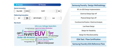
Samsung certified Ansys Redhawk-SC and Ansys® Redhawk™ for its entire line of FinFET process nodes — including 14nm, 11nm, 10nm, 8nm, 7nm, 5nm and 4nm — and will collaborate closely with Ansys on upcoming nodes. This certification includes power integrity EM and IR-drop, statistical EM budgeting, thermal analysis and multiphysics solutions for multi-die integration. Redhawk-SC verifies massive 4nm designs by executing signoff algorithms on its underlying Ansys® SeaScape™ infrastructure — reducing simulation time from weeks to hours, while boosting modeling fidelity. Ansys® Totem™ is correspondingly certified for transistor-level custom designs.
"The certification of Ansys Redhawk-SC, Redhawk and Totem supports our joint customers in rapidly completing new designs with improved confidence by managing increased power integrity, reliability and thermal challenges," said Sangyun Kim, vice president at Samsung Electronics. "Through the long, trusted alliance between Ansys and Samsung, our customers build cutting-edge silicon innovations, satisfy demanding performance objectives and are primed for winning the race to market."
"Industry-leading FinFET processes enable customers to innovate faster, smaller and lower-power applications. However, new technology challenges require an advanced simulation-driven analysis platform to maximize performance and reliability," said Vic Kulkarni, vice president, strategy, semiconductor business unit at Ansys. "This newest certification reflects Ansys' deep, ongoing relationship with Samsung Foundry, enabling our mutual customers to continue to signoff and verify breakthrough products with confidence."
/ About Ansys
If you've ever seen a rocket launch, flown on an airplane, driven a car, used a computer, touched a mobile device, crossed a bridge or put on wearable technology, chances are you've used a product where Ansys software played a critical role in its creation. Ansys is the global leader in engineering simulation. Through our strategy of Pervasive Engineering Simulation, we help the world's most innovative companies deliver radically better products to their customers. By offering the best and broadest portfolio of engineering simulation software, we help them solve the most complex design challenges and create products limited only by imagination. Founded in 1970, Ansys is headquartered south of Pittsburgh, Pennsylvania, U.S.A. Visit www.ansys.com for more information.
Ansys and any and all ANSYS, Inc. brand, product, service and feature names, logos and slogans are registered trademarks or trademarks of ANSYS, Inc. or its subsidiaries in the United States or other countries. All other brand, product, service and feature names or trademarks are the property of their respective owners.
ANSS–T
/ Contacts
Media | Mary Kate Joyce |
724.820.4368 | |
| Annette N. Arribas, IRC |
724.820.3700 | |
![]() View original content to download multimedia:http://www.prnewswire.com/news-releases/ansys-multiphysics-solutions-certified-for-samsung-foundrys-entire-line-of-finfet-process-technologies-301160157.html
View original content to download multimedia:http://www.prnewswire.com/news-releases/ansys-multiphysics-solutions-certified-for-samsung-foundrys-entire-line-of-finfet-process-technologies-301160157.html
SOURCE Ansys


